4. Dopant Barrier <불순물 장벽>
- 산화층이 실리콘 표면에서 성장하면 불순물 물질이 wafer로 들어가는 곳에 창을 생성시키기
위해서 Mask 개방으로 SiO2를 식각, 이때 산화물은 dopant의 확산으로부터
silicon의 표면을 보호.
- 선택적인 dopant의 도핑가능
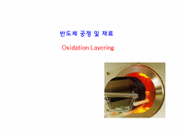
5. 금속층 사이의 유전체
oxide의 불안정한 상태 때문에 Ge보다는 Si 사용한 MOSFET(Metal Oxide Semiconductor Field Effect Transistor)이 반도체산업의 중심에 서있다. 이러한 MOSFET의 바탕이 되는 MOS를 이용한 capacitor 즉 MOS capacitor는 유전체로써 oxide를 사용하였기 때문에 붙여진 이름이며 이번 실험에서 제작할 소자이다. 전기신호의 증폭과 스
Oxidation of Graphite
What happens to Graphite?
Nanochannels or micropores are made.
Effects of Mild Oxidation.
Micropores acts as ‘reservoirs’ for lithium ions storage.
Prevent the graphite anode from expanding by lithium ion intercalation
Si has theoretical capacity of 4200mAh/g
Due to it’s large volume change, pulverization can be occurred.
Silicon has high-
3. a-IGZO기반
Oxide
TFT문제점
채널층에서 발생하는 문제
① 대기 중 산소나 수분과
금속의 자유전자가 반응
=> 자유전자 감소
② 빛에 의해 정공이 생성 됨
=> 정공 증가
↓
전기특성 신뢰도 감소
Transistor Switching 원리
채널이 형성되어
Source와 Drain간에
전류가 흐르기
1. 연료전지의 기본원리
1839년 초에 윌리엄 그로브(William Grove)는 수소와 산소로부터 전기를 만들어내기 위해서 물의 전기분해를 반대로 뒤집음으로써 연료전지의 기본적인 작동원리를 발견하였다. 연료전지는 연료와 산화(酸化)제가 공급되는 동안 화학적 에너지를 전기적인 에너지로 연속적으로
문턱전압은 0.7V가 일반적입니다. 저희 실험값은 3.7V가 나왔는데 좀 크게 나온것을 알 수 있씁니다.
Mobility 값은 300K 실온에서 Si 실리콘에서 전자 채널 형성되었을 때의 mobility값 1350보다 작은 값이 나왔습니다
Subthreshold swing 값은 일반적인 값인 0.1(저는0.07로알고있는뎋ㅎ) 보다 크게나왔습니다.
Converts sunlight directly into electricity
Non polluting
Long lasting sources of energy
No need of maintenance
In the long run, solar electricity is cheaper
Electrons of dye absorb solar energy
Electrons of dye are excited & Generate electron-hole pairs
Electrons transfer from dye to FTO via TiO2
1/2 I3- + e 3/2 I- at counter electrode
3/2 I- 1/2
oxide layer, it causes entire curve of graph to shift to the [Figure 12] C-V graph shift by direction of bias
side. These charges are generated by ions came in the process of deposition of oxide layer. When the charges exist in between the substrate and interface, the value of Vfb and C-V curve will shift by amount of the charge divided by Cox of Ci. The amount of shifting decreases as the posit
4. Equipment
4.1 RCA cleaning
RCA cleaning is a series of rinsing procedure prior to experiment with Si wafer. The purpose of the RCA clean is to remove organic contaminants (such as dust particles, grease or silica gel) from the wafer surface. There are three steps to be performed. The first step is to remove organic contaminant from surface of wafer. Second step is to remove any oxide layer
2. 이론
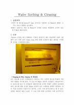
Pattern 공정을 하기 위해서는 주변의 청정도가 매우 중요한데, 아래 그림에서 보는 것과 같이 Clean room 에서 빛에 노출되지 않는 환경을 구비한 후 공정을 시작하여야 한다.
◦ Cleaning & Wet-Station 의 중요성
모든 반도체 공정은 오염물들의 근원이고 이는 소자의 성능과 수율에 직접적인